Open
a
better
future

Business
Semiconductor materials
Semiconductor materials
Innovative materical for Future Semiconductor
DS Techopia is leading the development of advanced materials that enable high-performance semiconductor manufacturing.
DS Techopia leads the industry to change by supporting the advancement of fine process technology.
Value Chain
-
01
 Wafer
-
02
 Oxidation
-
03
 Photolithography
-
04
 Etching
-
05
 Deposition(Thin Film)
- Deposition
- The process of creating thin films that serve to separate, connect, and protect circuits
-
06
 Metalization
-
07
 Testing
-
08
 Packaging
Main Usage
Precursor used in Thin film and Deposition processes during semiconductor manufacturing, used for thin film formation in semiconductor DRAM and Nand Flash memory production processes.
HCDS Hexachlorodisilane
01
Physical Properties
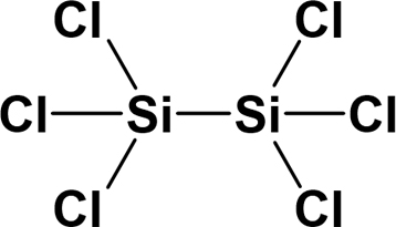
- Molecular Formula
- Si2Cl6
- CAS Number
- 13465-77-5
- Molecular Weight
- 268.88 g/mol
- Boiling Point
- 144 ℃
- Melting Point
- -1 ℃
- Density
- 1.58 g/mL at 0 ℃
- Physical State
- Colorless Liquid
02
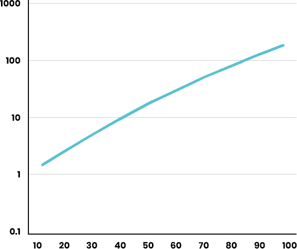
Vapor Pressure Curve
03
Application
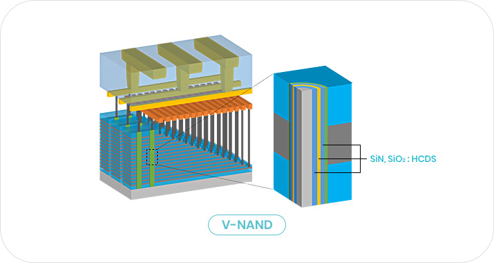
- Memory : SiN, SiO2, SiON Deposition Layer
SiCl4 Silicon tetrachloride
01
Physical Properties
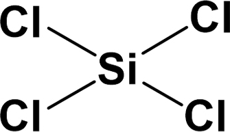
- Molecular Formula
- SiCl4
- CAS Number
- 10026-04-7
- Molecular Weight
- 169.9 g/mol
- Boiling Point
- 57 ℃
- Melting Point
- -68.7 °C
- Density
- 1.480
- Physical State
- Colorless liquid
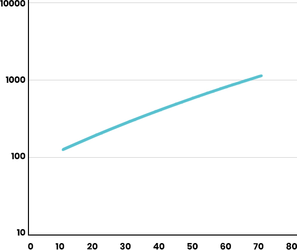
02
Vapor Pressure Curve
03
Application
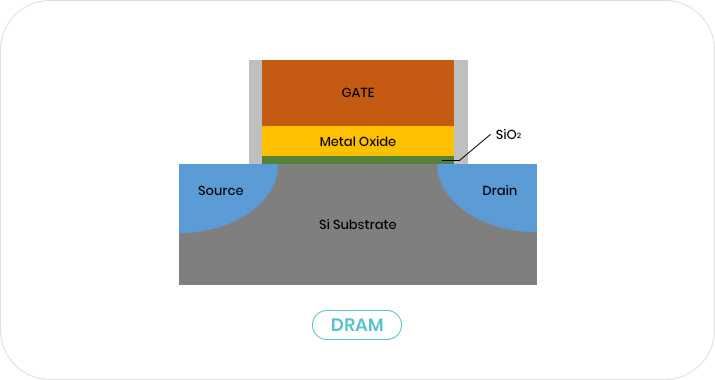
- Memory : SiN, SiO2 Deposition Layer
OMCTS Octamethylcyclotetrasiloxane
01
Physical Properties
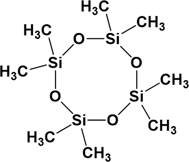
- Molecular Formula
- C8H24O4Si4
- CAS Number
- 556-67-2
- Molecular Weight
- 296.62 g/mol
- Boiling Point
- 175.8 ℃
- Melting Point
- 17.5 ℃
- Density
- 0.956g/mL at 25℃
- Physical State
- Colorless liquid
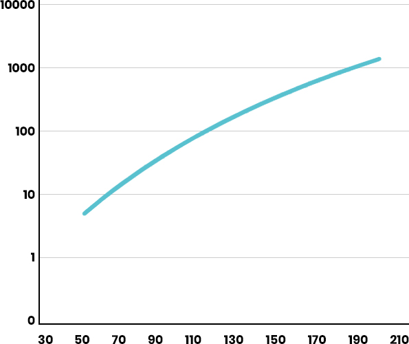
02
Vapor Pressure Curve
03
Application
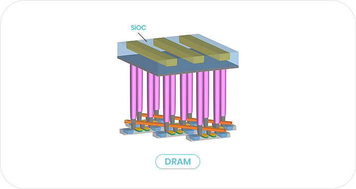
- Memory : Low-k Deposition Layer
Star-Ti Trimethoxy(pentamethylcyclopentadienyl) titanium(IV)
01
Physical Properties
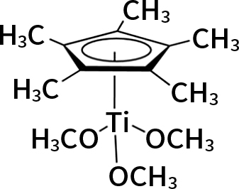
- Molecular Formula
- Cp*Ti (OMe)3
- CAS Number
- 123927-75-3
- Molecular Weight
- 276.19g/mol
- Boiling Point
- 285 °C
- Melting Point
- -
- Density
- 1.081
- Physical State
- Yellow Liquid
02
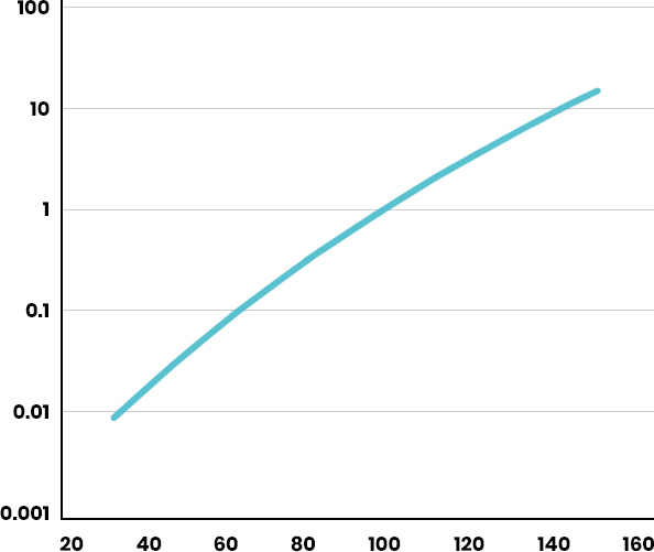
Vapor Pressure Curve
03
Application
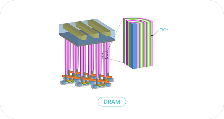
- TiO2 Deposition Layer
Strength
Why DS Techopia
-
Succeed in domestic produce of HCDS for the first time in Korea
-
Ultra-high-purity refinement and trace analysis technology tailored for semiconductor miniaturization and high integration.
-
Developing materials and canister analysis technology to meet customer needs
-
Continuous R&D Investment for New Future Materials Market
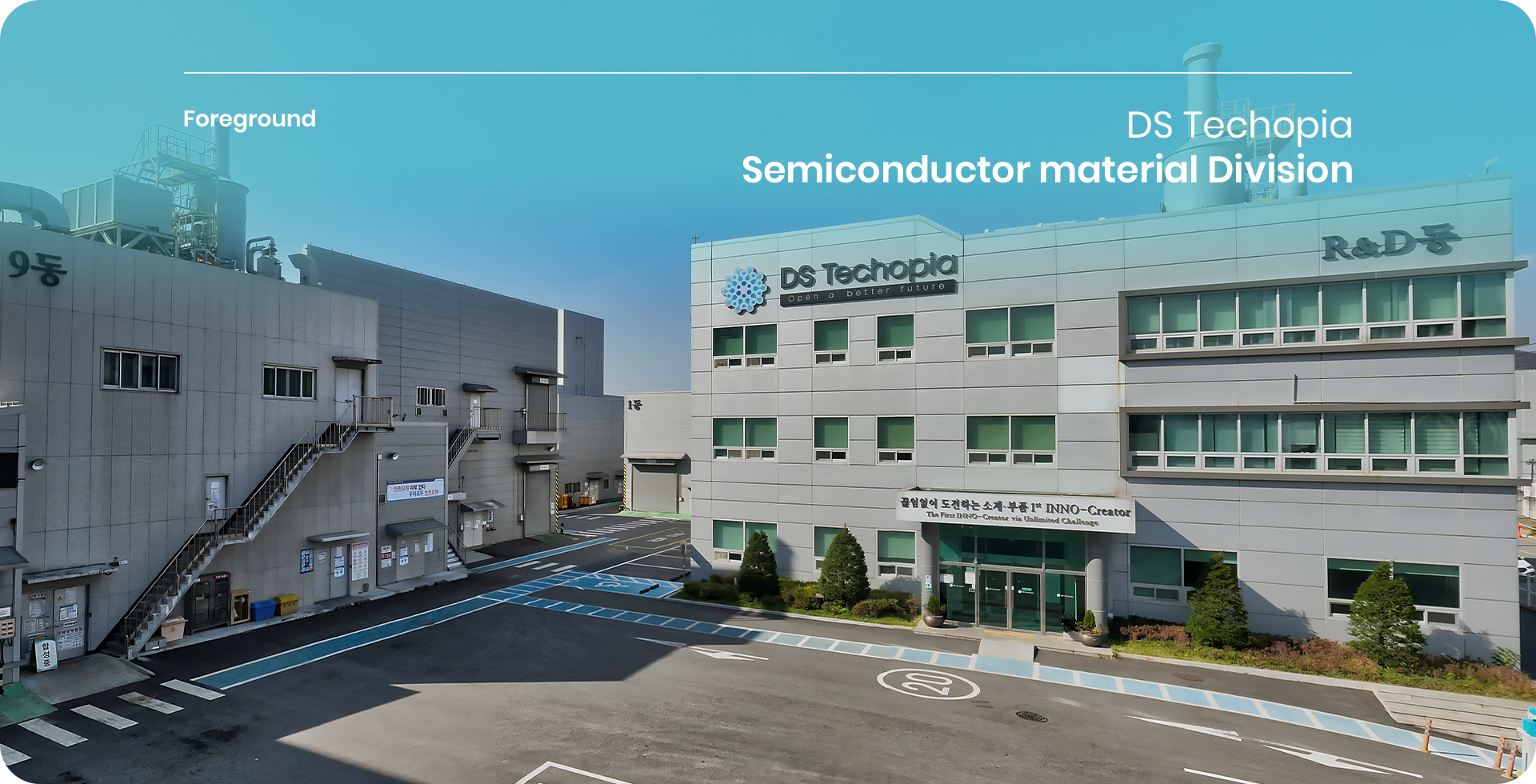
DS Techopia Semiconductor material Division
- Address.
- 30, 5sandan 3-ro, Seongnam-myeon, Dongnam-gu, Cheonan-si, Chungcheongnam-do, Republic of Korea
- Tel.
- 041-629-8200
- Fax.
- 041-564-5660

- DP Materials Business Division(HQ)
- 39, Pungsesandan 2-ro, Pungse-myeon, Dongnam-gu, Cheonan-si, Chungcheongnam-do, Republic of Korea
- Tel
- +82 41-903-9700
- Fax
- +82 41-903-9699
- Semiconductor Business Division
- 30, 5sandan 3-ro, Seongnam-myeon, Dongnam-gu, Cheonan-si, Chungcheongnam-do, Republic of Korea
- Tel
- +82 41-629-8200
- Fax
- +82 41-564-5660
- Fine Chemical Business Division
- 210, Namgongjusandan-gil, Gongju-si, Chungcheongnam-do, Republic of Korea
- Tel
- +82 41-840-7200
- Fax
- +82 41-852-3070
Copyright ⓒ 2024 DS Techopia .ALL RIGHTS RESERVED